
International Business Machines (IBM) has disclosed a semiconductor development with the introduction of its sub-1 nanometer (nm) chip technology.
The design operates at the 0.7 nm node, which represents an engineering shift toward atomic-scale dimensions.
This architecture addresses the physical limitations facing traditional flat chip scaling by utilizing a three-dimensional (3D) structure.
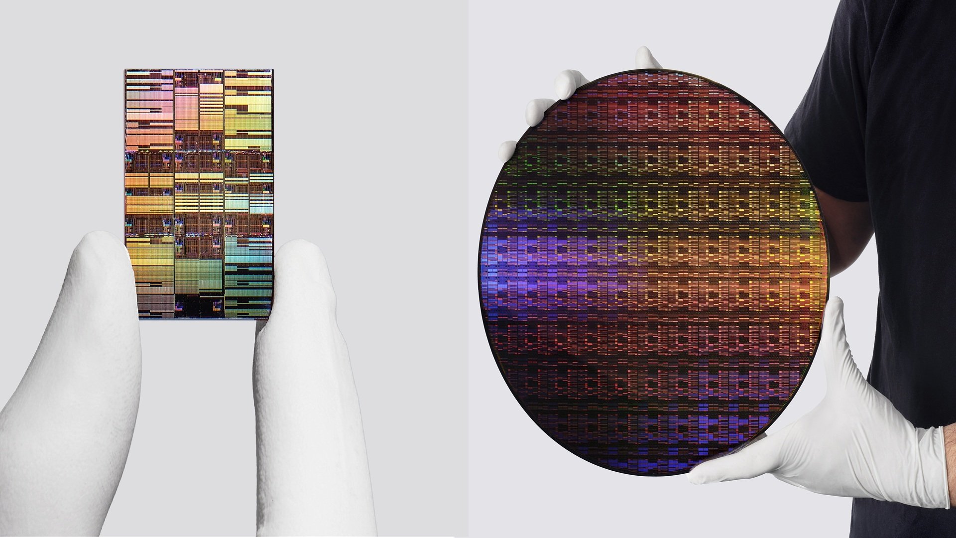
Researchers succeeded in placing nearly 100 billion transistors onto a piece of hardware roughly the size of a fingernail.
This represents double the transistor density achieved during the previous 2 nm breakthrough announced in 2021.
The configuration utilizes a proprietary design known as nanostack architecture.
Unlike conventional horizontal nanosheet designs, this approach stacks and staggers individual transistors vertically.
The vertical configuration leverages 3D sequential integration, allowing engineers to maximize space without expanding the physical footprint of the silicon.
According to initial technical documentation, the design yields up to 50 percent higher computing performance.
Alternatively, the architecture can deliver a 70 percent reduction in energy usage compared to current 2 nm technologies.
These adjustments allow chip designers to mix different material combinations within each individual layer.
Each layer can be tuned independently to optimize specific power and performance requirements.
The technology directly targets bottlenecks within modern Artificial Intelligence (AI) computing arrays and data centers.
High-performance compute clusters frequently face strict energy constraints and severe heat generation limits.
By improving the performance output per watt, the design allows facilities to expand processing capabilities without a matching increase in cooling infrastructure.
The development also alters the design of Static Random-Access Memory (SRAM), which remains crucial for rapid data access in advanced processors.
The new approach shrinks necessary memory cell sizes by approximately 40 percent.
On-chip memory scaling typically lags behind logic transistor shrinkage, creating data transfer bottlenecks.
Addressing this memory constraint is vital for supporting larger specialized processors used in machine learning.
The architecture has achieved experimental validation through ultra-thin dielectric bonding in Complementary Metal-Oxide-Semiconductor (CMOS) integration.
Engineers confirmed functional dual-channel engineering along with basic switching operations in functional CMOS inverters.
The physical integration process involves depositing material layers atom by atom to maintain structural integrity.
While the blueprint is complete, commercial production remains several years away.
The company estimates that the earliest market adoption of the technology will take at least five years.
The firm does not operate its own commercial fabrication facilities.
It collaborates with external manufacturing organizations, including its Japanese foundry partner, Rapidus.
Testing and development continue at a dedicated research complex located in Albany, New York.
The facility is scheduled to integrate a High Numerical Aperture Extreme Ultraviolet (High NA EUV) lithography tool.
The equipment, built by ASML, prints ultra-precise circuit pathways necessary for sub-1 nm logic scaling.
Development partners include Lam Research Corporation to refine materials and fabrication techniques.
The industry has moved away from using nanometer designations as direct physical measurements.
Modern process node names function as a shorthand for density and efficiency generations.
The 0.7 nm label designates a technical generation rather than the exact size of every component.
This structural transition is expected to sustain development trajectories for another decade.
Foundries will eventually utilize this baseline to scale designs down toward a single angstrom.
Comments (0)
Leave a Comment
No comments yet. Be the first to share your thoughts!